How PN junction is formed? Semiconductor for You
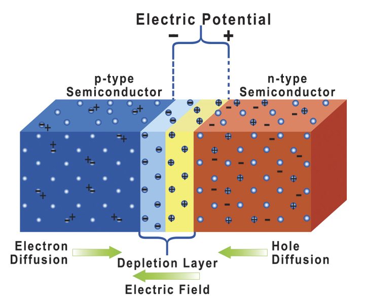
Definition: A P-N junction is an interface or a boundary between two semiconductor material types, namely the p-type and the n-type, inside a semiconductor. In a semiconductor, the P-N junction is created by the method of doping.
The PN Junction Solidstate Device Theory Electronics Textbook
A p-i-n diode is a p-n junction with an impurity profile tailored so that an intrinsic layer, the " i region," is sandwiched between a p layer and an n layer. The p-i-n diode has found wide application in microwave circuits.

PN Junction Diode and VI Characteristics Explained YouTube
Definition: A PIN diode is an advancement of normal PN junction diode. It is a 3-layer device in which an intrinsic layer i.e., undoped semiconductor is sandwiched between P and N regions. Thus, making it a PIN diode. The presence of intrinsic region exhibits high resistance property.
Complete Guide to PN Junction Diode [Updated] Characteristics
A PIN diode is a variation on a pn junction diode with a region of intrinsic semiconductor (the I in PIN) between the p-type and n-type semiconductor regions. The properties of the PIN diode depend on whether there are carriers in the intrinsic region. The PIN diode has the current-voltage characteristics of a pn junction diode at low.

Pn Junction Diode Working Principle Animation Ppt
A Pin diode is a special type of diode that contains an undoped intrinsic semiconductor between the p-type semiconductor and n-type semiconductor regions. It differs from a normal diode in the sense that it has an extra layer in between the p and the n junctions.

PN junction diodes (LIV) M Dash Foundation C Cube Learning
PIN diode Structures J.Y. Wah, C. J. Hepburn Overview A p-i-n diode is a p-n junction with a doping profile tailored so that an intrinsic layer, the 'i region,' is sandwiched between a p layer and an n layer. In practice, however, an idealized i region is.
Diode Physics
A PIN diode is a diode with a large and undoped intrinsic semiconductor region which is wedged between a p-type and an n-type semiconductor region. Since they are used for ohmic connections, the p-type and n-type regions are usually highly doped. In comparison to a standard p-n diode, this diode has a large intrinsic field.
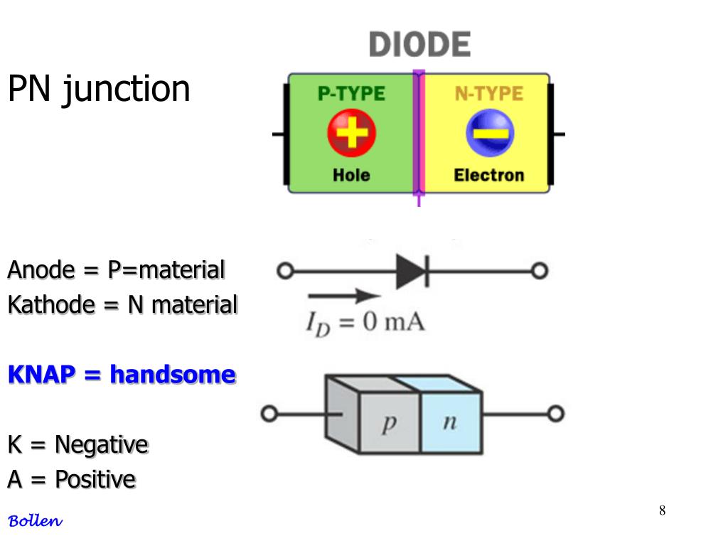
PPT PN Junction / DIODE PowerPoint Presentation, free download ID6537047
The PIN diode is a type of photodetector used for converting the light energy into the electrical energy. The intrinsic layer between the P and N-type regions increases the distance between them. The width of the region is inversely proportional to their capacitance.
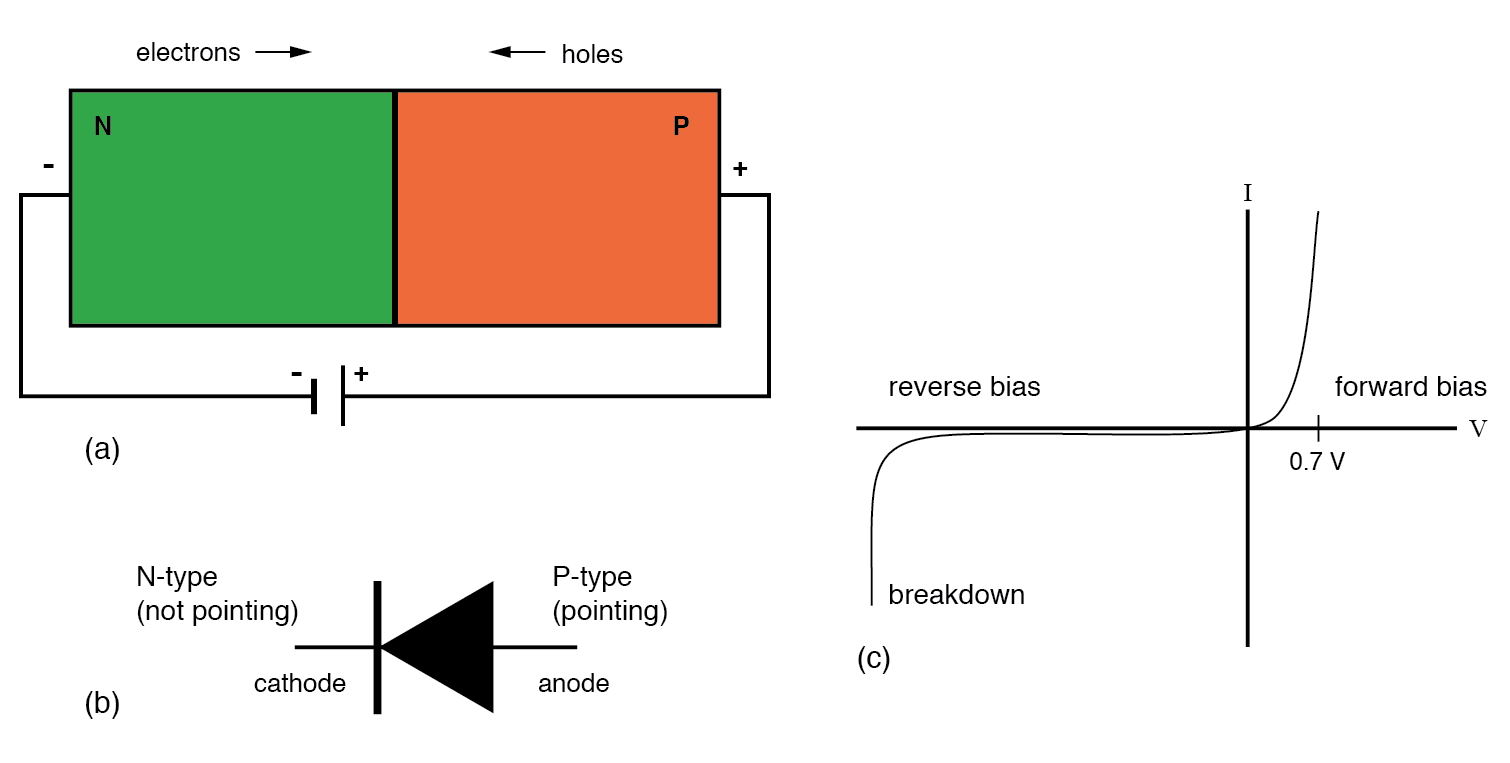
PN Junction Diode Formation, Symbol, Biasing, VI Characteristics, Application » ElectroDuino
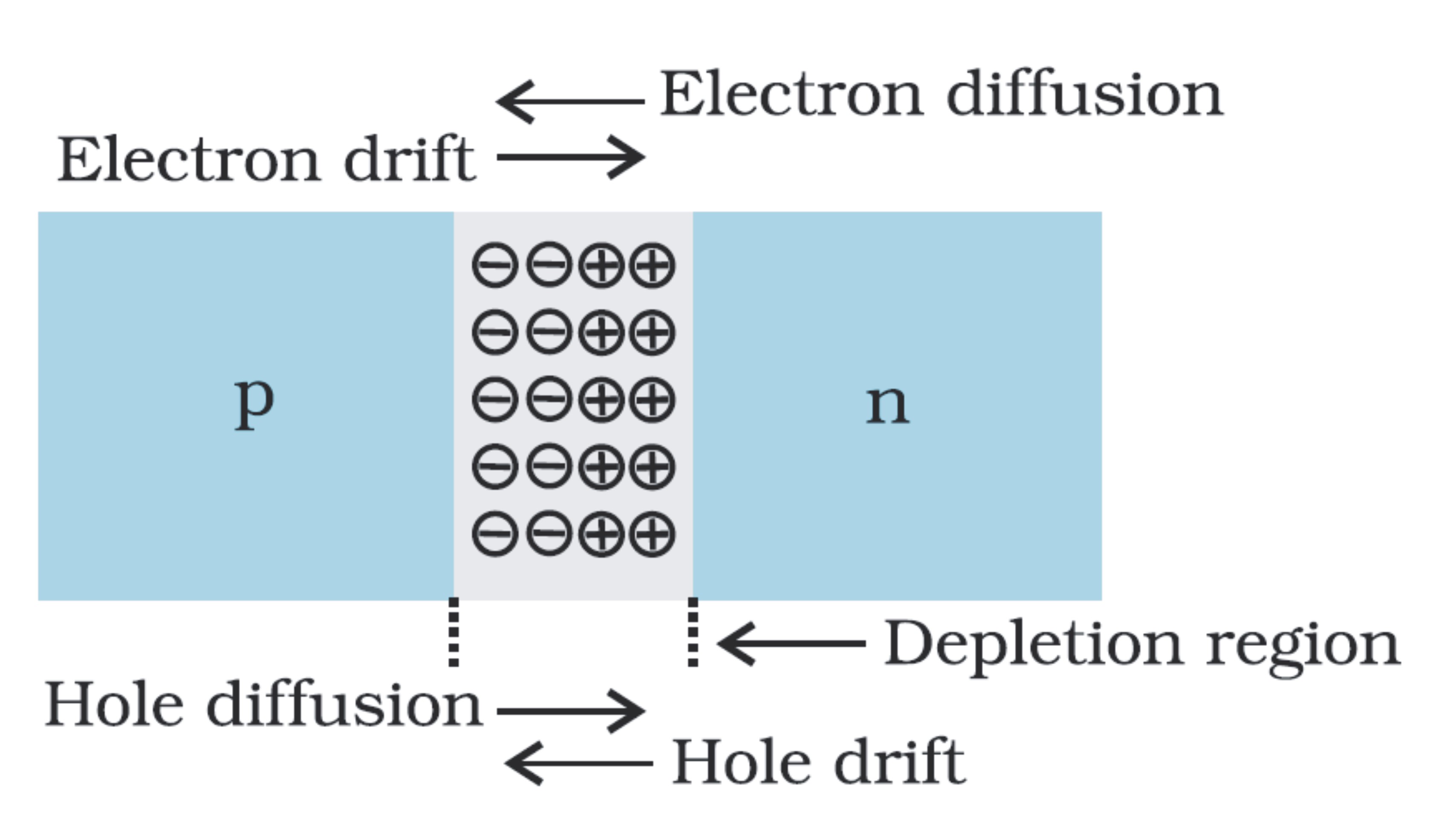
A p-n junction. The circuit symbol is shown: the triangle corresponds to the p side. A p-n junction is a boundary or interface between two types of semiconductor materials, p-type and n-type, inside a single crystal of semiconductor. The "p" (positive) side contains an excess of holes, while the "n" (negative) side contains an excess of electrons in the outer shells of the electrically.
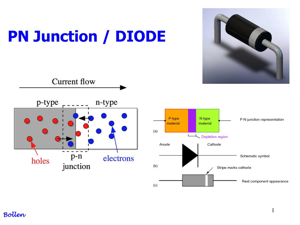
PPT PN Junction / DIODE PowerPoint Presentation, free download ID6537047
A PIN diode is a type of diode having undoped intrinsic semiconductor region placed between two regions called p-type semiconductor and the n-type semiconductor region. These two regions are primely heavily doped as they find applications for ohmic contacts. Characteristics of Pin Diode
pn Junction Diode Definition, Formation, Characteristics, Applications
The PIN diode is a one type of photo detector, used to convert optical signal into an electrical signal. The PIN diode comprises of three regions, namely P-region, I-region and N-region.

How A Pn Junction Diode Works Dr Bakst
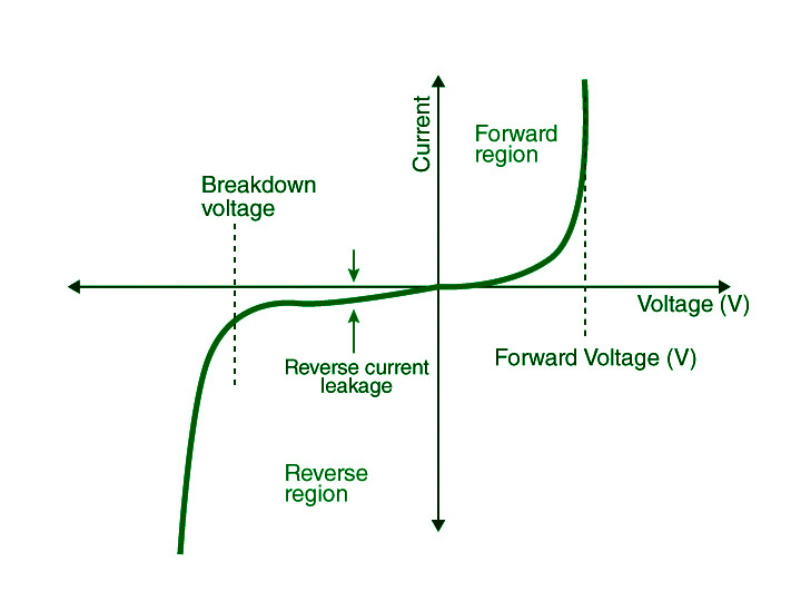
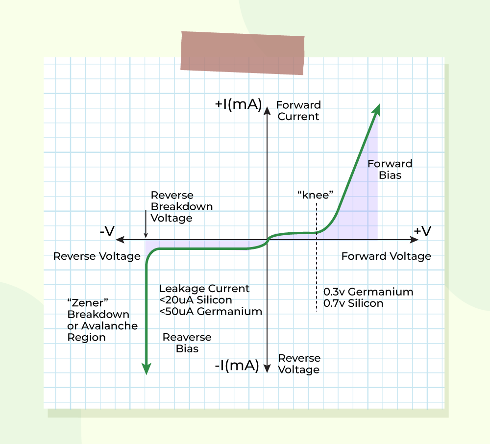
The pn Junction Diode -- Uses: Rectification, parts of transistors, light-emitting diodes and lasers, solar cells, electrically variable capacitor (varactor diode), voltage reference (zener diode) Depletion region & junction capacitance I-V characteristic Circuit applications and analysis Reference Reading

PN Junction Diode 1N4007 (pack of 10) Online India Circuit Uncle
No matter what you love, you'll find it here. Search Pin Diode and more. Looking for Pin Diode? We have almost everything on eBay.
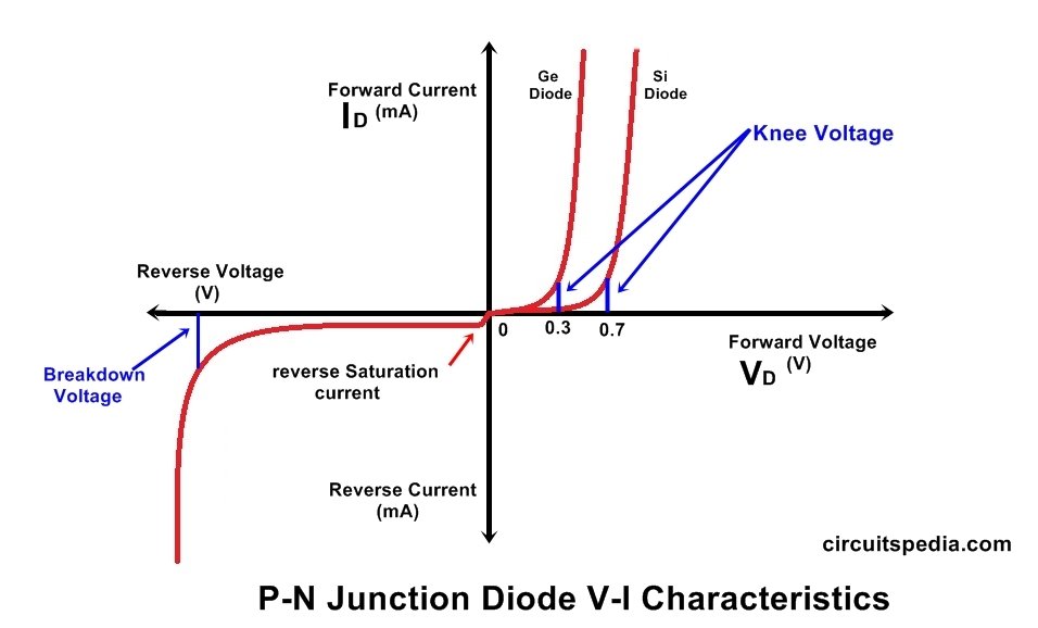
Semiconductor PN Junction Diode Working PN diode VI characteristics
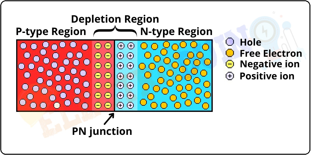
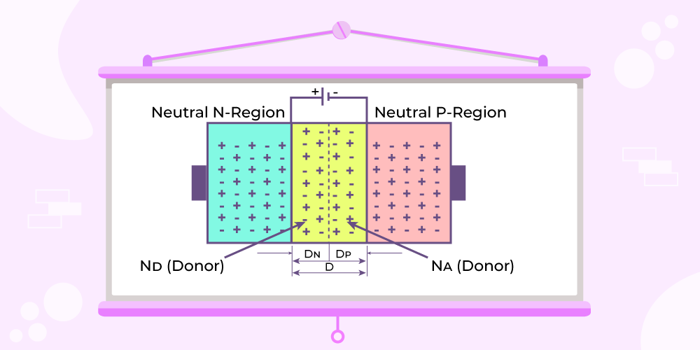
A PN-junction diode is formed when a p-type semiconductor is fused to an n-type semiconductor creating a potential barrier voltage across the diode junction The PN junction diode consists of a p-region and n-region separated by a depletion region where charge is stored.

How A Pn Junction Diode Works Dr Bakst
P-N Junction. Inside a semiconductor, a p-n junction is an interface or a border between two semiconductor material types, namely the p-type and the n-type. The semiconductor's p-side, or positive side, has an excess of holes, whereas the n-side, or negative side, has an excess of electrons. The doping process is used to produce the p-n.
pn Junction Diode Definition, Formation, Characteristics, Applications
January 18, 2021 by Electricalvoice Pin diode is a type of diode that has p-type and n-type semiconductor material sandwiching an intrinsic layer. The intrinsic layer is a layer of undoped semiconductor material. This is the structural difference between a normal PN junction diode and a PIN junction diode.